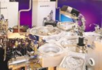
|
Etching Area:Etching is to remove the redundancy electric pattern on wafer surface by chemical or physical method. The area where etching is implemented is called Etch Area. |
|
 |
Thin-film Area:The area to deposit "dielectric layer" and "metal layer" as the conducted or insulated films, also has CMP (Chemical-Mechanical_Polish) to planarize the chips on the wafer's surface and add high (low) temprature RTP (Rapid-Thermal-Process) to the wafer. |
|
 |
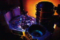
Diffusion Area:To diffuse the dopant into the wafer in high temperature furnance. By modifying the attribution, depth and PN interface square of dedicated area’s dopant, electric conductivity is adjusted to the right range. |
|
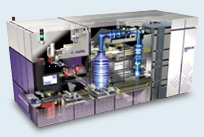 |
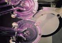
Photo Area:This area transfers circuit pattern from mask onto silicon wafer, which is coated by photo resist. Ultra high-resolution camera (Stepper or Scanner) is utilized here. And similar to a photographic darkroom process, yellow lighting environment is required to avoid unwanted exposure. |
|
2004 - 2026 , HeJian Technology (SuZhou) Co., Ltd.